Chip giant TSMC on Monday unveiled a new packaging platform for high-performance computing and AI chips that uses silicon photonics to improve the interconnect.
Kevin Zhang, vice president of business development at TSMC, said during ISSCC 2024 __ IEEE International Solid-State Circuits Conference __ the technology was developed to increase the performance of AI accelerators, which can be done by adding more high bandwidth memory and chiplets.
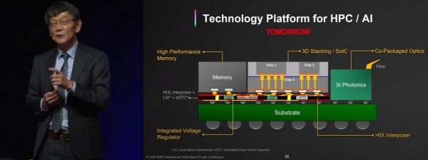
To add more HBM and chiplets, more interposers and chip-on-wafer-on-substrate must also be added, which can cause issues with the interconnect and power supply.
TSMC’s new packaging technology, through silicon photonics, uses fiber instead of I/O to transmit data, Zhang explained. The VP didn’t mention when the technology will be commercialized.
Another interesting factor of the technology is that heterogeneous die is stacked on the base die.
The packaging technology will apply hybrid bonding on the dies to maximize the I/O. Chips and HBMs will be mounted on the interposer, likely a local silicon interposer.
Zhang also said that the packaging will use an integrated voltage regulator to handle the issue of power supply.
The VP said the most advanced dies today can house up to 100 billion transistors but for AI, 3D packaging technology can increase this to 1 trillion transistors.
