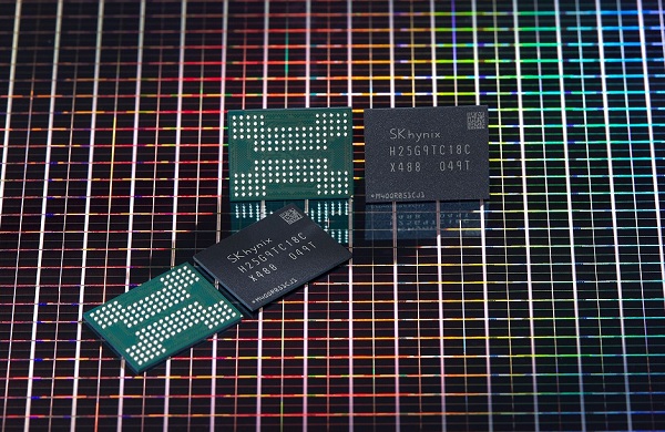
SK Hynix said on Monday that it has developed a 176-layer 512Gb triple level cell (TLC) NAND flash memory.
More dies can be produced per wafer, the company said, which allowed for an increase in bit productivity of 35%.
The chip uses charge trap flash (CTF) and peri under cell (PUC) technologies that the company began using for 96-layer NAND flash chips that allows for the production of “4D” products such as its latest chip, SK Hynix said.
Read speed in cell increased by 20% compared to its predecessor, while data transfer speed reached 1.6Gbps.
SK Hynix will launch a solution aimed at mobile devices that uses the latest NAND sometime in mid-2021. The chip aimed at mobile devices will have the maximum read speed improved by 70% and maximum write speed by 35% compared to their predecessor, the company said.
The company will also use the NAND to launch solid-state drives (SSD) aimed at consumers and the enterprise afterwards.
It has already provided samples of the NAND to a controller company.
SK Hynix will also develop a 1Tb NAND flash memory to launch at a later date.