Firm to expand supply to memory customers

Applied Materials has touted its latest optical wafer inspection system that utilizes big data and artificial intelligence (AI) technologies in South Korea.
The company said at an online press event for South Korean media that it plans to expand its supply of its systems from foundry and logic to memory chips as well.
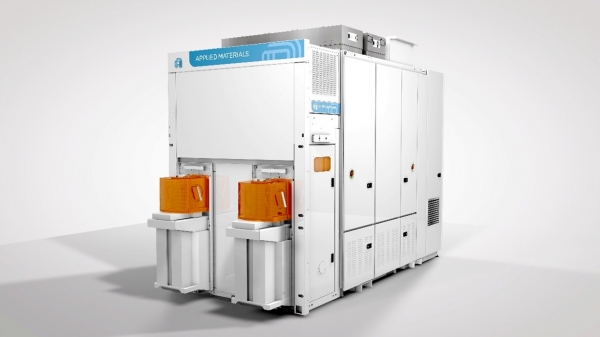
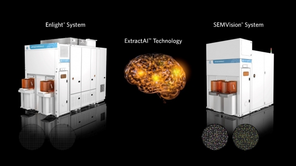
The new systems are Enlight optical wafer inspection system with the firm’s ExtractAI technology and SEMVision e-beam review system.
Applied Materials Korea senior director Lee Suk-woo said the new systems will reduce chip development and lead time for semiconductor firms.
Application of complicated technologies such as 3D transistors and multi-patterning technologies had increased the time it takes to find defects and fix them, and the new systems will help resolve this, Lee said.
Enlight is a high-resolution, high-speed inspection system. It can add inspection steps in a production process while also using big data to predict potential causes of lower yield rates. These additions will allow chip makers to monitor their lines better, Applied Materials said.
The company claimed the use of the system can save the cost of finding critical defects by a third compared to systems of its competitors. Enlight also supports both bright field and gray field in image collection.
Lee said Applied Materials spent five years in collecting data and technology development for Enlight, which was first launched in 2019. It has so far accumulated US$400 million in sales since launch as was the fastest selling product in the company’s history, the senior director said.
Extract AI technology is used to locate the defect that can cause reduction in yield rate out of millions of signals and noises produced by optical wafer inspection systems. The filtering algorithm allows engineers to secure manageable amount of data set, Applied Materials said.
Extract AI can be paired with Enlight. It can find the cause of defect through reviewing only 0.001% of the problem area, the company said.
The e-beam on SEMVision is used to classify specific yield rate signals and big data. The classified data is trained using an AI algorithm. This allows chip customers to accelerate chip production and yield rate improvements.
SEMVision G7 system can be synced with the new Enlight system and Extract AI.
Applied Materials was the only company to offer real-time connection between three such technologies, Lee said. This allows them to offer optimized process systems to its customers, he said, adding that the company plans to expand supply of these systems from foundry and logic to memory chip customers going forward.


