Samsung Display and its parent company Samsung Electronics are reviewing potential use of an underused liquid crystal display (LCD) plant in South Korea, which could possibly result in the plant being converted to a semiconductor plant, TheElec has learned.
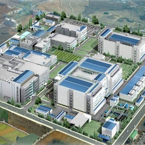
The plant at Cheonan, owned by Samsung Display, currently houses multiple buildings that were built to manufacture LCD panels. The around 500,000 meter-square plant was built in 1996. It houses two buildings, L3/L4 and L5/L6, which were used to manufacture small to mid-sized LCD panels. These building currently house the A1 line, Samsung’s first line for OLED production that is currently partially operating. The building also house a line for LCD color filters and Samsung SDI’s small battery line.
However, since Samsung Display has announced that it was exiting the LCD business, the plant is not being used for any large-scale production.
The Cheonan plant costs Samsung tens of billions of wons per year (equivalent tens of millions of dollars) in maintenance fees and taxes, a source told TheElec.
Samsung was not selling the plant despite its low use as the company could convert the plant to manufacture semiconductors, the source said. It takes a lot of approval processes from local governments and residents to build an entirely new facility, but the Cheonan plant could be used right away if need be as it is already built, the source said.
L3/L4 had been used by Samsung Electro-Mechanics as a panel level package (PLP) factory back in 2018. L5/L6 was rented by Samsung Electronics, with the purpose of converting it to a wafer level package (WLP) factory. At the time, Samsung Electronics and Samsung Electro-Mechanics planned to convert the Cheonan plant into a major base for its package production. However, Samsung Electro-Mechanics is currently facing difficulty in developing advanced packaging technology and securing customers. Its current operation rate for existing packaging facilities are also below 100%. In 2019, Samsung Electro-Mechanics sold its PLP operation to Samsung Electronics.
Samsung Electronics isn’t considering any additional investments into the Cheonan plant to expand its package operations, other people familiar with the matter said. However, the tech giant has recently extended is lease to use the Cheonan plant this year, they said.
Meanwhile, Samsung Electronics’ semiconductor business unit conducted a working survey of the Cheonan plant to determine whether it could be used as a foundry fab. Cheonan plant can house over two 300mm foundry lines equivalent to the size of the S1 line at Giheung. But the source said the working survey was done to review just one of many options Samsung is considering for the plant at Cheonan. L5/L6 was built to handle Gen 6 (1500x1800mm) display panel substrates, which makes it quiet large __ enough to house 300mm wafer equipment. However, Samsung’s working survey showed that the building will need additional construction to add in earthquake resistance design and other upgrades. The reminaing building, L3/L4, will need to be demolished and any new fab to replace it will need to be built from scratch, the survey showed, according to the source.
To convert the Cheonan plant into a semiconductor fab, Samsung Display will also need to transfer the A1 line for OLED production and Samsung SDI’s small battery line, to a different plant or close them down. Currently, A1 line manufactures automotive OLED panels.
World’s largest chip foundry TSMC is planning to expand its 28-nanometer (nm) production capacity by 100,000 to 150,000 300mm substrates in the next two to three years, Taiwanese media The Economic Daily reports.
The global foundry industry’s shortage in capacity cause many products to face production problems, the source said. Amid this climate, Samsung was seriously considering expanding its 14nm and 28nm capacity that is more lucrative over advanced processes such as 5nm and 7nm, they added.