Lam Research on Thursday announced new etching solutions that can be used for gate-all-around (GAA) transistor structures in wafers.
The solutions were already in use by Samsung for its 3-nanometer (nm) GAA process, the company said.
They were being manufactured by Lam Research Manufacturing Korea, the manufacturing subsidiary of Lam Research in South Korea.
GAA uses four sides as current channels, unlike FinFET which uses three.
Fabricating them requires extremely precise etching while not damaging other layers on the wafer.
Lam said its etch solutions provide ultra-high, tunable selectivity and damage-free material removal required to support advanced logic nanosheet or nanowire formation, enabling chipmakers such as Samsung to make the next evolutionary leap from planar to three-dimensional structures for DRAM as it reaches its planar scaling limit.
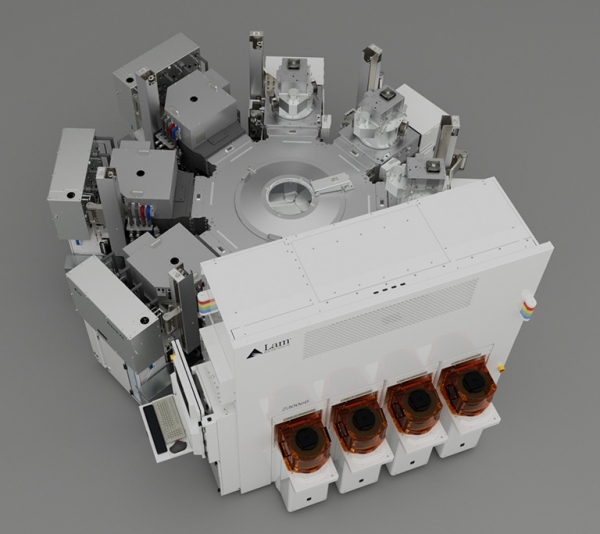
The solution comes in three tools; Argos, Prevos and Selis.
Argos comes with what Lam calls Metastable Activated Radical Source technology. It can selectively modify and decontaminate wafer surfaces precisely for optimal performance.
Prevos offers atomic layer precision, ultra-high selectivity etching for oxide, silicon, and metal. Lam said this was done by combining new chemistries and vapor technology with agile temperature control.
Selis, meanwhile, uses both radical and thermal etching with uniform top to bottom process control without damaging the wafer structure, the equipment maker said.
Prevos and Selis can also be offered as one integrated tool for flexibility and improved queue time control, the company added.