Samsung on Friday said it will spend 20 trillion won by 2028 to build a new chip research complex at its campus in Giheung, South Korea.
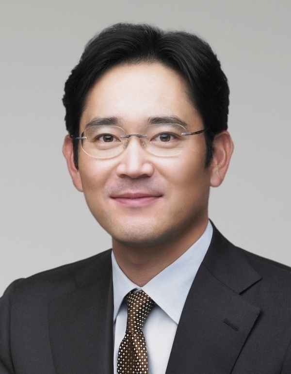
The groundbreaking ceremony was attended by Samsung vice chairman Lee Jae-yong, who stressed that the company’s chip business wouldn’t exist if it didn’t emphasize technology and invest preemptively.
It was Lee’s first official activity as vice chairman of Samsung since he received a presidential pardon last week for his bribery conviction.
The planned research complex at Giheung is aimed at making advances in its memory, system semiconductor and foundry technologies.
The complex is planned to be Samsung’s most advanced so far, the South Korean tech giant said.
It will take up 109,000 meters square of space at Giheung campus and run an R&D line starting in 2025 before the complex’s completion in 2028.
Samsung stressed that Giheung is where it developed the world’s first 64Mb DRAM, which allowed the company to become the world’s largest DRAM producer in 1992 and the world’s largest memory chip maker in 1993.

