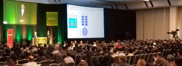
SPIE Advanced Lithography Digital Forum will be held online next month from February 22 to 26.
SPIE, the international society for optics and photonics, will host the event that will showcase extreme ultraviolet (EUV) lithography technology that is growing ever more important in semiconductor production.
Companies in the field such as Intel, ASML, Applied Materials, Samsung Electronics and SK Hynix will attend the conference as speakers.
The Forum will discuss: EUV lithography; novel patterning technologies 2021; metrology, inspection, and process control for semiconductor manufacturing; advances in patterning materials and processes; optical microlithography; design-process-technology co-optimization; advanced etch technology and process integration for nanopatterning; and advanced lithography product demos.
Plenary event will start with presentation by Michael Mayberry, retired CTO of Intel. His talk will be titled: The future of compute: how the data transformation is reshaping VLSI.
This will be followed by presentation of John Hu, Director of Advanced Technology at Nvidia, titled: A new era for AI HPC and IC technologies in the transition to an intelligent digital world.
Presentations will also be given on topics such as EUV, optical lithography, measurement, etching and others.
EUV equipment maker ASML will introduce its next-generation EUV platform that increased NA to 0.55 from 0.33.
KLA will showcase method and technology to overcome test coverage difference. Applied materials will showcase new deposition and etching technologies that can increase density of DRAM. Ram Research will show off a EUV photoresist system for dry etching and Nikon will share the latest development in optical exposure technology.
Samsung Electronics will take part in three sessions as chair: EUV lithography; metrology, inspection, and process control for semiconductor manufacturing; and advances in patterning materials and processes.
Samsung will share its plasma technology for APMI and lens-less EUV mask inspection technology. The conglomerate will share reflection measurement method for semiconductor material measurement and high-speed wafer film measurement using optical sensor systems. The company will also share flattening of high-temperature carbon hard mask and metal purifiers for lithograph materials.
Lim Changmoon, head of SK Hynix’ future technology, will chair the session for EUV scanner roadmap. This session will introduce lithography technology for higher NA as well as mass production.
Nextin will share its research called: comparative near infrared through-focus scanning optical microscopy for 3D memory subsurface defect detection and classification. Intel’s TSOM application in its 3D NAND flash will be discussed at the session. Nextin’s inspection equipment Iris also uses TSOM technology.

