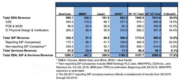
Sales of semiconductor electronic design automation (EDA) and IP hit US$3.157 billion in the first quarter, an increase of 17% from a year ago, according to SEMI.
It is the highest growth since 2011.
Spending in the sector also increased. In the first quarter, it was shown that 49,024 people were hired in the EDA and IP space, an increase of 6.7% from the same time period a year ago.
EDA tools are used to design the layout of semiconductor circuits and printed circuit boards.
Demand for them are increasing as more and more chips are being designed to handle AI, machine learning, high performance computing, 5G and autonomous driving applications.
In the back-end process of semiconductor production, the rising demand for wafer level package has also increased the use of EDA.
In IP, due to process nodes becoming smaller, use of outsourced IPs are also increasing.
Cadence, Synopsys and Siemens EDA control over 70% of the market share in EDA tools. Cadence and Synopsys also provide IPs. Other IP companies include Arm, Rambus and CEVA. In South Korea there is Chips&Media.
Per region, APAC, which excludes Japan but includes China, saw EDA sales increase 26.9% year-on-year to US$1.166 billion.
This is from Samsung and TSMC working with EDA companies on advanced process nodes.
Samsung is collaborating with Synopsys on 3-nanometer gate all around process. TSMC is planning to apply FinFET in 3-nm.
Meanwhile. China, despite seeing EDA and IP sales increase 73% last year, is seeing sales drop this year due to US sanctions that is blocking access to US software.
In the US, sales increased 15% year-on-year to US$1.285 billion. Europe, Middle East and Africa saw sales increase 14% to US$447 million.

