In 1904, English physicist John Ambrose Fleming developed the first vacuum tube. The tube had a filament inside as well as a cathode and anode plates placed on either end of the glass tube. Electrons flowed between the two electrodes. Radios used in the early 1900s used such tubes. Despite being a historic invention, the vacuum tube didn’t lead to the development of the electronics industry. Long use of the tube would burn the filament. It also overheated. ENIAC, the first computer, used vacuum tubes and emitted great amounts of heat and light. This would attract moths, which reportedly caused constant short circuits.
After close to a half a century has passed since the vacuum tube was developed, in the winter of 1947, the transistor was developed at Bell Labs. The transistor had a smaller design __ no glass tubes, no heat and no vulnerable filaments. Its switching speed in the mean time was 20 times faster. They were small and easy to produce, while being less prone to errors. Transistor allowed for smaller, cheaper electronic products. But for complex tasks, multiple transistors were required. This led to the development of integrated circuit (IC) in 1958. Multiple transistors were integrated into one chip. IC paved the way for accelerated expansion of the electronic industry.

Transistor density race begins
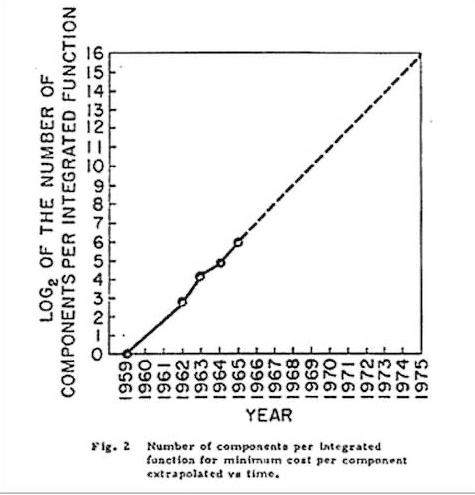
IC provided the rule of the game in the semiconductor industry. Intel co-founder Gordon Moore wrote an article called Cramming more components onto integrated circuits on the then prestigious journal Electronics Magazine. The now famous Moore’s Law started from the piece.
Moore argued that the increase in transistor density in an IC would lead to steep drop in manufacturing costs. He argued that roughly every year, the number of transistors on microchips will double. He said by 1970 that manufacturing cost would drop to one tenth of their equivalent in 1965. Moore altered his observation slightly in 1975, posting that the number of transistors will double every two years. Packing in more transistors in the same space increase the chips performance and consumes less power. And most importantly, as Moore posited, chips can be made at lower costs. So started the semiconductor industries competition to increase the number of transistors in their chips in a bid to surpass rivals and to secure more profits.
In 1993, the Semiconductor Industry Association (SIA) made the National Technology Roadmap for Semiconductors (NTRS). It was an attempt to foster collaboration between the equipment, material and component companies in the semiconductor industry. In 1998, SIA became closer with its counterparts in Japan, South Korea, Taiwan and Europe and created the International Technology Roadmap for Semiconductors (ITRS). The entire global industry followed the roadmap. But with the publication of ITRS 2.0 in May 2016, ITRS has not updated the roadmap. This was because it believed that the gate length could no longer be made shortened in the 2020s. IEEE’s International Roadmap for Devices and Systems in the meantime continued offer updates and published white papers, but the organization also believes it will be difficult to reduce gate length after 2024.
The problem with “nanometer”
So will semiconductor microfabrication stop after 2024 when 3-nanometer chips are set to be launched? The short answer is no.
However, we must go over the nanometer terminology used in the industry that is suppose to give an idea on the technological level of chips. Semiconductors have a structure where electric current flows from the source to the drain. There is a gate between the two that acts as switches to either let the current flow or block it. In the past, the industry measured the gate length and called a chip “made with 90 nanometer process node” or “65 nanometer process node.” The nanometer referred to the length of the gate.
Now those in the industry and academia are calling for the end of using the nanometer terminology.
This is because, due to the intensifying competition and marketing purposes, what companies call nanometer no longer refers to the minimum physical gate length. This discrepancy only increased more after TSMC and Samsung, for their 16-nanometer and 14-nanometer nodes, respectively, began adopting FinFET 3D structures for their gates.
Hanyang University professor of materials science and engineering Jinho Ahn told TheElec that the numbers used by semiconductor companies to refer to the “technology generation” of their products, from 10-nanometer, 7-nanometer to 5-nanometer, has actually no longer any relation to the actual minimum gate length of their real products.
Rino Choi, professor of new materials science and engineering at Inha University, also shared a similar view with TheElec. In the past, each generation of process nodes became smaller by 0.7 times each time (90-nanometer, 65-nanometer, 45-nanometer, 32-nanometer, 22-nanometer and so on), this rule ended starting in the 10-nanometer range. Companies began calling their process nodes by smaller numbers despite the actual gate length not becoming smaller. The companies would use new structures or new materials and claim that they offer “equivalent scaling” __ that is, and equal affect to the gate length shortening. Companies are increasing chip performance and density using different technologies as the gate length itself is increasingly becoming difficult to achieve, Choi noted.
This has caused problems and confusion. For example, what TSMC and Samsung each call “10-nanometer node” have different integration levels. The pair’s 10-nanometer is thought to pack 50 million transistors, while what Intel calls 10-nanometer pack 100 million transistors.

LMC density metrics to the rescue?
Last year in April, nine scholars from MIT, Stanford, Berkeley and TSMC published a paper called A Density Metric for Semiconductor Technology on IEEE.
“Since its inception, the semiconductor industry has used a physical dimension (the minimum gate length of a transistor) as a means to gauge continuous technology advancement. This metric is all but obsolete today,” they wrote.
“As a replacement, we propose a density metric, which aims to capture how advances in semiconductor device technologies enable system-level benefits. The proposed metric can be used to gauge advances in future generations of semiconductor technologies in a holistic way, by accounting for the progress in logic, memory, and packaging/integration technologies simultaneously.”
LMC stands for logic, memory and connectivity. LMC is divided into DL, DM and DC __ density of logic transistors, bit density of main memory and density of connections between the main memory and logic.
The writers said the LMC density metric can serve as a “common language” so that the semiconductor industry can communicate with customers, consumers and investors clearly. Use of terms such as nanometer could give the wrong impression that technology advancement is reaching its limit, they said.
The semiconductor industry is yet to offer a roadmap after 3-nanometer. Do they not have one? Or are they mulling over the terminology they wish to use. Either way, the use nanometer may end after 3-nanometer. Time will tell.