ASML’s highly anticipated high-NA EUV equipment will begin shipping in 2024 and cost between 300 to 350 million euros per unit, CEO Peter Wennink said in a conference in Seoul on Tuesday.
High-numerical aperture (NA) extreme ultraviolet (EUV) is an upgraded version of the Dutch company’s prior EUV equipment. The NA is increased from 0.33 to 0.55, allowing it to draw even finger circuit patterns which is necessary for the development of 2-nanometer (nm) or below process nodes.
Wennink said high-NA EUV equipment will be applied to fabs for the first time in 2024 and the company plans to manufacture 20 units per year in the long term.
Despite the high price tag, most chip makers have already expressed their strong interest in applying the equipment.
Intel last year had said it already placed an order; TSMC has also confirmed this.
Samsung and SK Hynix have not publicly confirmed this but sources said they have already placed orders with ASML as well.
Given that Wennink had said the company will manufacture around 20 units per year, supply will likely be short compared to demand.
Chipmakers are likely to compete fiercely with each other to receive delivery of the equipment first.
The ASML CEO said the company will be able to mass-produce the equipment sometime between 2026 and 2027 and will work to expand its production capacity as much as possible.
On the global chip market, Wennink said while the short-term downturn is continuing in the mid- to long-term the market can only grow.
For the next ten years, the market is expected to grow 9% per year on average, he said, while it will be worth between 1 trillion to 1.3 trillion dollars in 2030.
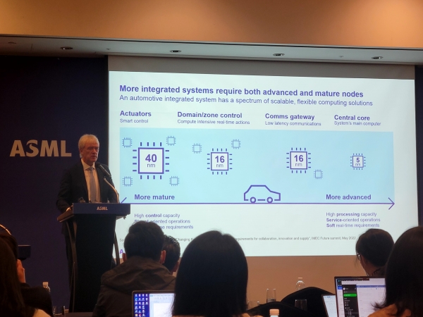
The automotive sector, while it uses mostly chips made with legacy process nodes, is also expected to shift to the use of smaller chips going forward, he added.
More cars are becoming digitized and this will cause the application of 40nm to 5nm chips in them going forward, Wennink said.
Meanwhile, the CEO this week is in Seoul to mark ASML’s plan to spend 240 billion won to build its semiconductor cluster in the city of Hwaseong, home to one of Samsung’s major fabs and local chip companies.