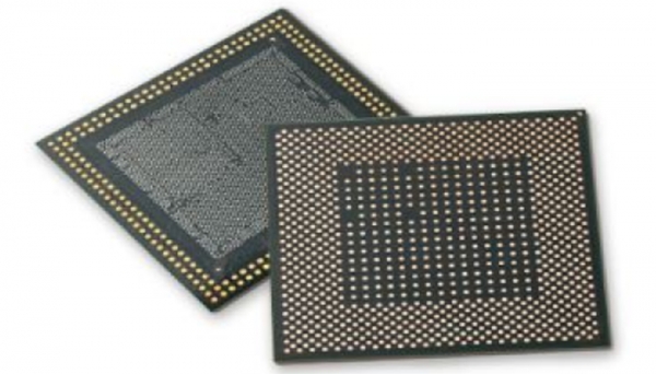
Samsung Electro-Mechanics has brought down the line width/line spacing (L/S) of its chip package down to 5 micrometers.
This was to respond to an increase in I/Os of chips, Samsung Electro-Mechanics group head Woo Seok Yang said during the SMT&PCB Tech Conference hosted by TheElec in Suwon, south of Seoul.
The latest generation will offer a 10/10um line width with a 20um pitch while the next generation package will have 5/5um, Yang explained. Samsung Electro-Mechanics plans to follow up 5/5um with 3/3um or 2/2um, he added.
The time gap between each generation will be 18 months, Yang noted.
Besides narrowing the line width, improving the cu roughness of the insulator layers and circuits was also important, the group head said.
Controlling the precision of the roughness of the insulator layer allows the microcircuits to be wired properly while improving the roughness of the circuits can minimize signal losses, he said.
The increase in I/Os of chips means the bumps mounted on the package must become even smaller. Yang said a bump pitch of 40 to 50um will be needed and package and board companies like Samsung Electro-Mechanics needed to respond to this.
The via that connects the layers must also become narrower and the company will use equipment with extremely short wavelength to achieve this, he added.

