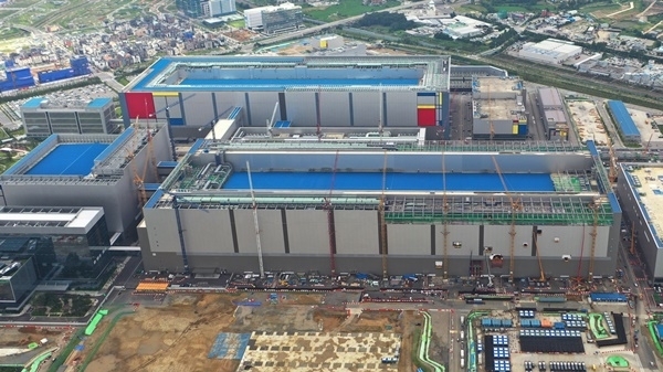
Samsung Electronics’ second factory at its Pyeongtaek semiconductor plant has begun mass production, the company said.
It will produce 3rd generation 10-nanometer (nm) LPDDR5 mobile DRAM using the extreme ultraviolet (EUV) process, Samsung said.
The factory, called Pyeongtaek Line 2, is being designed to produce DRAM and NAND Flash memories as well as logic chip for clients.
In May, Samsung began construction for the EUV contract chip making line there. In June, it began building the 3D V-NAND Flash line. Both lines will go live in 2021.
Samsung has been building the Pyeongtaek campus since 2015. The first factory, called Pyeongtaek Line 1, began mass production in June, 2017. Construction for Pyeongtaek Line 2 began on January, 2018.
Pyeongtaek Line 2 spans 128,900 square meter and is the world’s largest chip production line, Samsung said.

Next-gen LPDDR5 mobile DRAM
The 16Gb LPDDR5 mobile DRAM Samsung has begun producing is the first memory product to be made using the EUV process.
In February, the company began producing its predecessor, the 2nd generation 10nm LPDDR5 DRAM.
The new DRAM, when combined to a x64 16GB package, boasts speeds of 51.2GB/s.
Samsung said its 6,400Mb/s speed per chip is 16% faster than its predecessor 12Gb LPDDR5 mobile DRAM, which had a speed of 5,500Mb/s.
The new memory will be supplied to global smartphone makers for their new flagship products, the company said.
Samsung will also secure reliability in high temperature for the new memory so that it can be applied to automobiles.

